
Inledning
In the highly sensitive world of semiconductor manufacturing, where even a minor environmental fluctuation can compromise millions of dollars’ worth of product, precise control over production conditions is non-negotiable. Among the most critical environmental parameters are temperature and humidity. This is where temperature and humidity transmitters come into play. These devices continuously monitor and transmit accurate data, ensuring stable environmental conditions throughout every phase of semiconductor production.
This article explores the vital roles these transmitters play in semiconductor facilities—from cleanroom control to equipment protection—and highlights their irreplaceable value in ensuring product quality, yield, and operational efficiency.
The Critical Role of Environmental Conditions in Semiconductor Manufacturing
Semiconductor devices are made at microscopic scales where moisture, heat, and airborne particles can introduce defects or reduce yield. To avoid this, production environments—especially cleanrooms—are held to strict environmental standards.
Humidity, if left uncontrolled, can lead to condensation or electrostatic discharge (ESD), both of which can damage delicate wafers or integrated circuits. Likewise, temperature fluctuations can affect equipment performance, alignment, and the chemical reactions involved in photolithography, etching, and doping.
This level of precision requires a reliable and real-time environmental monitoring solution—temperature and humidity transmitters.
Applications of Transmitters in Semiconductor Facilities
a) Cleanroom Climate Control
Cleanrooms in semiconductor fabs typically operate under strict ISO Class 5–7 standards, where even minor fluctuations in temperature or humidity can disrupt critical processes. Temperature and humidity transmitters serve as the backbone of climate control, providing real-time data to building management systems (BMS) or HVAC systems. This enables automated adjustments to air handling units, humidifiers, and dehumidifiers to maintain stable conditions.
Maintaining cleanroom environments at approximately 21–23°C temperature and 40–55% RH is crucial for several reasons:
Preventing condensation on wafers and tools that could lead to short circuits or corrosion
Minimizing electrostatic discharge (ESD), which can damage sensitive microelectronic components
Ensuring dimensional stability of photomasks and substrates, which are highly sensitive to humidity-induced expansion or contraction
High-accuracy transmitters help maintain these narrow environmental windows, ensuring cleanroom compliance and reducing risk in highly sensitive production areas.
b) Photolithography Rooms
Photolithography is one of the most environmentally sensitive stages in semiconductor fabrication. During this process, wafers are coated with a light-sensitive resist, exposed to UV light, and developed to form intricate circuit patterns. Even minor environmental fluctuations can result in critical defects.
Here, temperature and humidity transmitters play a vital role by enabling precise control over:
Resist coating uniformity, where variations in humidity can affect resist thickness
Pattern fidelity, as temperature deviations as small as ±0.5°C may lead to overlay errors or alignment drift
Focus stability, essential for high-resolution exposure tools
By continuously monitoring and adjusting environmental conditions, transmitters ensure:
Consistent critical dimension (CD) control
Higher process repeatability
Lower rates of rework or wafer rejection
In short, these sensors are key to protecting photolithography quality and maximizing throughput.
c) Etching and Deposition Chambers
Etching and deposition processes—such as plasma etching, chemical vapor deposition (CVD), and physical vapor deposition (PVD)—are typically conducted in sealed chambers under vacuum or controlled gas atmospheres. However, the surrounding room environment still plays an important role.
Ambient temperature and humidity can:
Affect chamber component temperatures, which may influence deposition rates or plasma stability
Impact equipment reliability, as high humidity levels may cause condensation in valves or sensors
Interfere with load-lock operations, where wafers move between vacuum and atmospheric conditions
Installing transmitters in the surrounding area enables engineers to:
Detect early signs of instability, such as temperature drift or humidity spikes
Optimize preventive maintenance, reducing downtime caused by environmental-related malfunctions
Maintain chamber consistency, indirectly improving yield and process uniformity
These transmitters thus serve as an extra layer of environmental assurance, even in controlled chamber operations.
d) Material Storage and Chemical Rooms
Many of the chemicals and raw materials used in semiconductor processes—such as photoresists, developers, solvents, and specialty gases—are hygroscopic, temperature-sensitive, or both. Improper storage conditions can degrade chemical integrity, impacting performance or safety.
Temperature and humidity transmitters are essential in these areas to:
Monitor critical storage parameters 24/7
Send alerts or trigger alarms when environmental conditions deviate from safe ranges
Ensure compliance with manufacturer-recommended storage conditions for regulated materials
For example, photoresists typically require cool, dry storage to avoid premature degradation. Similarly, specialty gases must be kept at stable temperatures to maintain purity and pressure control. Accurate transmitters help facilities protect valuable inventory and reduce waste due to improper storage.
Benefits of Using Temperature and Humidity Transmitters
a) Real-Time Monitoring and Feedback
Transmitters provide continuous data to the central control system, enabling real-time monitoring. This allows for immediate corrective actions, preventing deviations from affecting production.
b) Improved Yield and Quality
By maintaining strict environmental conditions, these sensors directly contribute to reducing wafer defects, improving lithographic accuracy, and minimizing downtime—leading to higher yields.
c) Reduced Equipment Downtime
Environmental transmitters also help identify trends or abnormalities that could indicate equipment issues. By catching environmental anomalies early, facilities can avoid costly equipment damage and unplanned downtime.
d) Compliance with Industry Standards
Semiconductor fabs must comply with strict ISO and SEMI standards. Temperature and humidity transmitters support compliance by maintaining records and validating environmental control for audits and certifications.
e) Data Logging and Traceability
Modern transmitters can integrate with data logging systems for historical analysis and traceability. This is essential for root-cause analysis in case of product issues and supports continuous improvement efforts.
Choosing the Right Transmitter for Semiconductor Environments
When selecting temperature and humidity transmitters for semiconductor facilities, consider the following features:
–High Accuracy: Choose models with at least ±1% RH and ±0.2°C to ensure precise control in sensitive processes like lithography and etching.
–Snabb svarstid: Quick detection of environmental changes helps prevent defects and maintain yield.
–Långsiktig stabilitet: Low sensor drift reduces recalibration needs, ideal for continuous operation.
–Robust Design: Devices should resist chemical cleaners and EMI, common in cleanroom environments.
–Flexible Outputs: Support for both analog and digital signals allows easy integration with BMS, SCADA, and HVAC systems.
–Easy Calibration: On-site or remote calibration ensures long-term accuracy with minimal downtime.
These features help ensure reliable, high-quality monitoring tailored to the demanding needs of semiconductor environments.
Product Recommendation: Reliable Environmental Monitoring from HENGKO
Looking for a transmitter that meets semiconductor-grade standards?
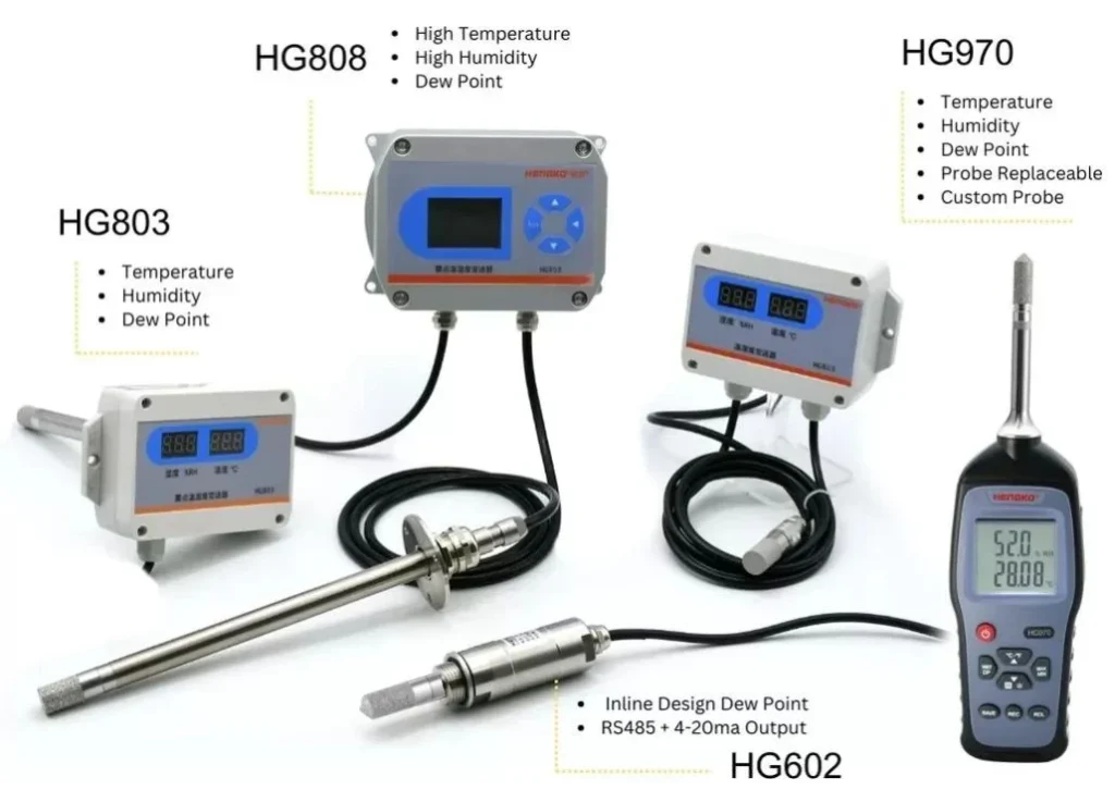
HENGKO’s HG808 Series Temperature and Humidity Transmitters are engineered for high-precision industrial environments. With high accuracy, rapid response, and strong anti-interference design, they are ideal for cleanrooms, photolithography areas, and precision equipment zones.
Kontakta oss på sales@hengkometer.com today to explore custom integration options and discover how our sensors can safeguard your semiconductor production.
Slutsats
As semiconductor production continues to push the boundaries of precision and miniaturization, environmental monitoring becomes more important than ever. Temperature and humidity transmitters are not just tools—they are essential safeguards that protect product quality, ensure consistent process outcomes, and keep operations compliant and efficient.
From cleanrooms to chemical storage, these sensors help semiconductor manufacturers maintain control, reduce risk, and stay ahead in a competitive industry. Investing in reliable environmental transmitters is an investment in long-term manufacturing success.